
Click here to see other posts about XPS
Only 10 $ for interpretation of each element in your XPS spectrum
Payment Upon Completion

Send your spectra...
Principle
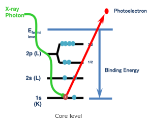
X-ray Photoelectron Spectroscopy (XPS) or Electron Spectroscopy for Chemical Analysis (ESCA) is a technique which analyzes the elements constituting the sample surface, its composition, and chemical bonding state by irradiating x-rays on the sample surface, and measuring the kinetic energy of the photoelectrons emitted from the sample surface. XPS instrument using Al Kα rays can generally obtain information on elements within a few nms of the sample surface.

Additionally, the change in bond energy (chemical shift) caused by the electron state surrounding the atoms to be analyzed, such as atomic valence charges and interatomic distances, tend to be greater than the chemical shift observed in AES, which makes the relative ease with which the state of chemical bonds can be identified another advantage of XPS.
 |  |
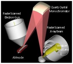
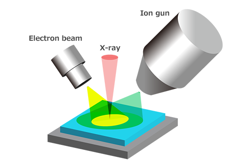
A scanning micro-focus x-ray source is an x-ray source that can scan a focused monochromed Al Kα beam on the sample. In general, characteristic x-rays such as Al Kα rays and Mg Kα rays are widely used as excitation sources for photoelectrons. The x-ray beam diameter can be set between several µmφ to several hundred µmφ, and the scan range can be changed arbitrarily, enabling measurement of the most appropriate analysis area for the sample. Secondary electron image observation (SXI: Scanning X-ray Image) based on this feature also allows for quick and accurate analysis location designation. Additionally, it supports various analyses including multi-point simultaneous analysis, large area measurement, line analysis, and area analysis.
Charge compensation mechanism (dual beam charge neutralization)
XPS is used for element/chemical state analysis for a wide range of solid samples from conductive to insulating materials. However, with insulating material samples, a positive charge occurs in the x-ray irradiated area due to the generation of photoelectrons. A spectrum measured in a positively charged state shifts to the high bond energy side (low kinetic energy side) compared to its actual position, making it difficult to grasp the correct energy position. Thus, with insulating material samples, charge neutralization is necessary during measurement. The dual beam technique, which irradiates a low energy electron beam and an ion beam simultaneously, is a neutralization method which stabilizes uneven charges on the surface in a self-repairing way, and is capable of stable charge neutralization for a wide range of insulating materials. It is also an essential feature for microscopic area analysis.
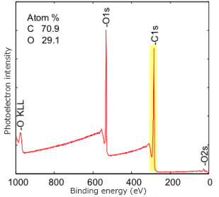
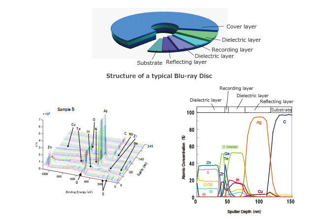
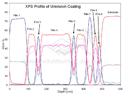
Since the information depth measurable with XPS is in the range of several nms from the surface, when the surface contamination layer is thick, or when evaluating a deeper area, ion sputtering is used to perform surface etching. An element composition or chemical bonding state depth profile can be obtained from the spectrum information gained through alternating between sputtering and measurement. Depth profiles are used for film thickness evaluation of samples with a multilayer structure and cause analysis for discoloration/corrosion of metal. Generally, argon (Ar) ions are used for depth profile analysis for inorganic materials such as metals and semiconductors while fullerene (C60) and argon gas cluster ions (Ar-GCIB) are used for organic materials, so different sputter ion guns are used depending on the material and purpose.
X-ray photoelectron spectroscopy (XPS Analysis) also called Electron
Spectroscopy for Chemical Analysis (ESCA) is a chemical surface
analysis method. XPS measures the chemical composition of the outermost
100 Å of a sample. Measurements can be made at greater depths by
ion sputter etching to remove surface layers.
All elements except for H and He can be detected at concentrations above 0.05 to 1.0 atom %, depending on the element. In addition, chemical bonding information can be determined from detailed analysis. Conductive and nonconductive samples can be measured and the technique is well suited for polymeric materials. The sampled area varies from 1 mm down to 30 µm in diameter.
X-ray Photoelectron Spectroscopy Analysis (XPS)
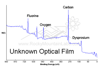
In XPS, also known as Electron Spectroscopy for Chemical Analysis (ESCA), X-rays bombard a sample creating ionized atoms and ejecting free electrons. The energies of these free electrons are related to their binding energies in the original atom. By measuring these characteristic energies, XPS Analysis identifies the chemical elements present in the sample. XPS provides both elemental and, to a certain extent, chemical information in the top 3-30 atomic layers (10-100Å) in solid samples. The sensitivity varies between 0.01-1 atom% dependent upon the element. It can do nondestructive depth profiling to 100 Å and detect all elements except H and He. Ion sputtering combined with XPS is used to accomplish deeper profiling. XPS is especially good for obtaining elemental surface composition of unknown materials, including conductors and insulators.
Critical problem solving with surface analysis is enhanced by reducing the probe area when using XPS Analysis. Small-spot XPS instruments probe for composition, chemistry, and contamination in 0.01 mm2 areas. It also makes XPS sputter depth profiles a reality.
One of the primary reasons for using XPS Surface Analysis to analyze samples is its inherent high surface sensitivity. This results from the fact that nearly all of the electrons which are used for analysis escape from only the outermost four to five atomic layers of the material. This high surface sensitivity permits the easy detection of most surface concentrated elements that would be undetectable by bulk or quasi-bulk techniques, e.g. XRD, XRF, EDS or Electron Microprobe. Remember, chemistry begins at the surface.
Imagine that a sample surface is contaminated by 20% coverage of Si from a silicone lubricant. Using XPS Analysis, the Si atoms represent ~6% of the atoms present in the 4-atom deep sampling volume. However, by using one of the bulk or quasi-bulk techniques, the Si atoms now represent ~0.03% or less of the >1 µm deep sampling volume. Given that surface Si concentrations as low as 0.10.% can be detected, the advantage of XPS over bulk techniques is readily apparent.
One very important reason for using XPS Surface Aanlysis is that it is nondestructive. XPS uses very soft (low energy) x-rays that produce minimum energy input to the sample during analysis. Electron beam analysis techniques concentrate a high amount of energy in a small region and can be very destructive toward organic materials or other thermally sensitive compounds. Bulk analysis techniques often require that the sample be powdered and placed in a matrix material introducing a high probability of altering or entirely losing some surface species.
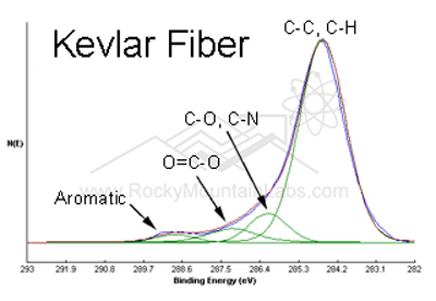
In addition to providing a detailed elemental surface composition, XPS Analysis provides even more information about the detected elements. Changes in the chemical environment or oxidation state of an atom can cause corresponding changes in the energies of the electrons that are ejected and analyzed. These energy shifts or “chemical shifts” have been well studied and tabulated for many different compounds. By measuring these shifts, it is possible in most cases to accurately assign the chemical environment of a given element.
Another important advantage of XPS over electron beam techniques, i.e. AES, Electron Microprobe, etc., is its ability to analyze insulating specimens with relative ease. Since the analysis beam (x-rays) does not consist of charged particles, the insulating specimen is not required to conduct away any charge buildup due to incidence of the analysis beam itself. The specimen is only required to conduct away enough charge to compensate for the small number of electrons which were ejected from the sample. This small positive charge buildup is easily compensated for by use of a “flood gun”, which directs low energy electrons to the sample surface.
In addition to the inherent advantages of using XPS generally, the small-spot instrument that Rocky Mountain Laboratories’ employs has a number of special features that give an enormous edge over other instruments. The sample transfer and sample chamber configuration allows the analysis of samples a s large as 3.75″ diameter x 0.375″ high. Or, many specimens may be mounted and measured by software automation, if they are of uniform size and shape. The minimum size is limited only by the size of the smallest x-ray beam (50 µm), which has been used to analyze a single 10 µm organic fiber.
The largest x-ray spot (image of the x-ray beam on the sample) is 1-2 mm and is used primarily for rapid data acquisition during survey scans. The smallest x-ray spot is most often used for analysis of small heterogeneous features on a larger sample or simply for analysis of a very small sample. Because the x-ray spot is smaller than in other XPS instruments, remarkably rapid and precise depth profiles are now routine, since both raster size and beam voltage of the ion etching gun can be greatly reduced.